Yamaha DX7 Technical Analysis
Foreword #
This article is intended to serve as an introductory technical analysis of the Yamaha DX7, detailing some of the known information about the synthesiser's engineering. This article doesn't intend to be an exhaustive repository of such information, or as reference material for technical means. Instead it intends to provide an informative overview of the subject.
The intended audience for this article is people with a software-engineering or similar technical background who are interested in the technical aspects of synthesisers.
Updates #
Since this article was originally published, in April 2021, much new research into the DX7's technical implementation has taken place. Ken Shirriff managed the incredible feat of
decapulsating the OPS chip, and analysing its functionality. This revealed, among other
things, the format of the internal sine, and exponential ROM tables; I was able to disassemble, and document
the DX7's firmware ROM, revealing many interesting technical details; Veteran audio-plugin designers Plogue released the groundbreaking
Chipsynth OPS7. Representing what is likely the definitive emulation of the DX7 to date; and some of
Yamaha's
internal documentation
about the DX7 surfaced. Providing some useful information about the synth's sound chips, and hardware.
This article has been updated to reflect these new developments.
Acknowledgements #
The debt of gratitude this article owes to the hard work of others is so great that I would be remiss to even risk taking undue credit for their efforts.
This article would not have been possible without the work of
Acreil, Raph Levien, the
Dexed team, and Steffen Ohrendorf. I would also like to thank
MadFame
for his fantastic research into the DX7's history.
Introduction #
In 1983 Yamaha Corporation released the now iconic DX7 synthesiser. Featuring a novel form of digital synthesis called frequency modulation, it would introduce musicians to a new world of sounds not previously possible with its analog contemporaries. Its characteristic brassy, metallic timbres would go on to define the sound of the decade. By all accounts it was revolutionary. It would go on to sell over 200,000 units worldwide, becoming the first commercially successful digital synthesiser.
The frequency modulation synthesis that forms the basis of the DX7 had its origins in the research of Stanford University professor John M. Chowning. Inspired by the groundbreaking work of Max Mathews at Bell Labs, Chowning shifted his course of study from music composition to focus on computer music. While experimenting with modulating a sound wave's frequency, Chowning discovered that as the frequency of the modulating wave increased into the audible spectrum, interesting harmonic partials appeared in the carrier tone, while still retaining the original note's pitch. He quickly realised this technique opened up a new world of tonal possibilities that contemporary analog synthesisers simply couldn't match.
The significance of Chowning's discovery was not lost on his colleagues, who urged him to patent this remarkable new technique1. With the help of Andy Moorer from Stanford's Artificial Intelligence Lab, Chowning would publish the groundbreaking paper The Synthesis of Complex Audio Spectra by Means of Frequency Modulation, and United States Patent No. 4,018,121.
In mathematical terms, FM synthesis is achieved by using the instantaneous amplitude of a signal (the modulator) to adjust the frequency of another signal (the carrier). This might make more sense when visualised:
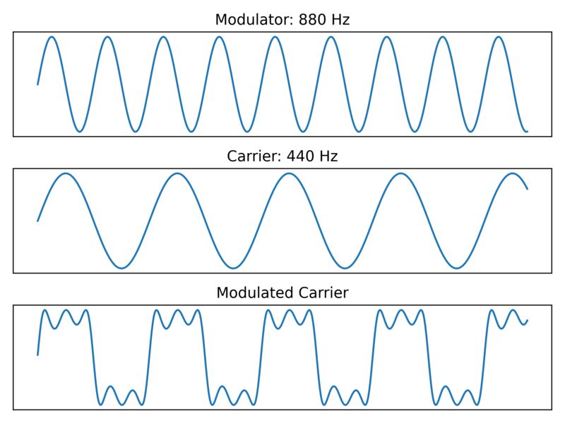
There are many fantastic resources online that give a much better explanation of FM synthesis than I can. Here is a particularly informative resource that I recommend. Another more mathematical approach to frequency modulation can be found here, created by composer and synthesiser pioneer Barry Truax.
By the mid-1970s, Stanford's Office of technology and licensing had yet to successfully find a prospective licensee for their breakthrough among American music technology manufacturers2. The investment required to pivot to digital technology was simply too big a financial risk to take for companies specialising in analog synthesisers. To find a licensee, Stanford would need to look abroad: Despite not having a significant market presence on American shores, Yamaha was at that time the largest manufacturer of musical instruments in the world. As fate would have it, one of their senior engineers —an expert in digital technology named Kazukiyo Ishimura— happened to be visiting their American branch at the time, apparently researching the very kind of integrated circuit technology that would make their future FM synthesis technology possible. He was willing to take a trip out to Stanford to hear Chowning's breakthrough for himself. In Chowning's own words: "In ten minutes he understood; he knew exactly what I was talking about" (Darter, 1985).
Impressed with what they saw, Yamaha would go on to purchase an exclusive license to the technology from Stanford. The rest is history. For more information about Chowning and Yamaha's collaboration, a fantastic documentary on the history of the DX7's development can be seen here, put together by the amazing synth historian, and patch creator MadFame
Roland Corporation's founder Ikutarō Kakehashi also met with Chowning to discuss his research. Unfortunately slightly too late to secure FM synthesis for Roland, with Stanford having signed an exclusive license with Yamaha only six months earlier. In his memoirs, Kakehashi admits that Yamaha were the right people for the job, given their capability to manufacture the LSI chips necessary to make the technology viable. (Kakehashi, 2002, pp. 194-195)
Roland's technical R&D director Tadao Kikumoto —himself no stranger to innovation, having been the inventor of the iconic TB-303— spent a year poring over Yamaha's technical literature looking for a way to implement an FM synth without running afoul of patent infringement3, He would also invest considerable time searching high and low for prior art that would invalidate Yamaha's patent. A search that would ultimately not prove fruitful (Reiffenstein, 2004, pp. 275-276). However unsuccessful these efforts may have been, Roland's research in the area of digital synthesis would ultimately lead them to produce their own groundbreaking digital synth: The D50.
Yamaha's approach to patenting their FM technology is by all accounts comprehensive. It's through these patents, service manuals, and the heroic reverse engineering efforts of some extremely talented engineers that we've been able to gleam what information we know of the DX7's internals.
Hardware #
The beating heart of the DX7 is a Hitachi 63B03RP microprocessor, an enhanced version of Motorola's 6800 series of 8-bit CPUs, built under license as a second-source supplier4. Clocked at around 1MHz, it provides the synthesiser a steady pulse, but not the kind of raw processing power required for real-time digital synthesis. The DX7's real capabilities lay inside two proprietary integrated circuits: the YM21280 FM-Operator Type S chip, otherwise known in Yamaha's technical literature as the OPS, and its counterpart the YM21290 Envelope Generator or EGS. As their names suggest, the OPS and EGS are responsible for operator and envelope generation respectively.
We know from the service manual that the OPS processes all 16 six-operator voices in ~20.368032μs. From this we can determine that the synth's overall sample rate is 49096Hz.
MIDI I/O is handled by the synth's CPU, while the scanning of the DX7's analog input (keyboard, foot pedal, and panel switch events) is handled by a separate "sub-CPU", a Hitachi 6805S 8-bit processor. The sub-CPU communicates with the synth's analog peripherals via a multiplexed A/D converter, and transmits this data to the main CPU via one of its IO ports using a complex handshake mechanism described in detail in the service manual.
The DX7's smaller desktop module cousin, the TX7, has an entirely different design. It features a different microprocessor, the Hitachi HD63A03, and does not include a sub-CPU. All input scanning is performed by the main processor. The TX7's service manual —an incredibly detailed source of technical information— provides a memory map for the CPU, as well as a flowchart of the serial interrupt routine, timer interrupt routine, and main executive loop. The DX7's budget-oriented counterpart, the DX9 would also make do without the DX7's sub-CPU.
YM21280 #
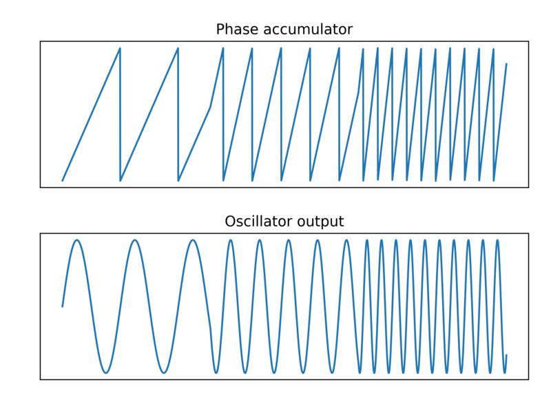
Each of the DX7's six operators consist of a digital sine wave oscillator, with its own independent envelope. In technical terms, these are known as numerically controlled oscillators: A phase accumulator register is used to store an index into a lookup table of wave amplitude values stored in ROM. In this system the angular velocity of the oscillator's wave is controlled by incrementing the phase accumulator each sampling iteration with an amount proportional to the desired frequency. This implementation forms the basis of Direct Digital Synthesis, a technique used in a variety of different engineering disciplines.
The YM21280's pre-calculated sine wave lookup table is stored in logarithmic format. Using a novel mathematical trick known to anyone familiar with a slide-rule, storing the oscillator's wave data in logarithmic format allows for scaling the wave's amplitude without the need for multiplication5. Given the logarithmic identity: log(xy) = log(x) + log(y), storing the operator's wave and envelope data in logarithmic form allows for replacing the multiplication of the wave's amplitude with the envelope gain with a relatively cheap addition operation. To convert the product of this calculation from logarithmic to linear format, the OPS stores a lookup table of exponential values.
The remarkably talented Ken Shirriff has been able to decapsulate the YM21280, and reverse-engineer its internal implementation. From his amazing research, we know that the OPS' sine ROM uses a clever delta encoding mechanism to reduce the amount of die space needed to store the lookup table. The full details of which are available in his blog. He has also been able to demonstrate that the final format of the sine table is a 14-bit fixed-point representation.
Taking full advantage of the sine wave's symmetrical property, the OPS stores only a quarter of the sine's full period. This quarter can be flipped and mirrored to assemble the full sine wave. Ken Shirriff's decapsulation on the OPS chip verified that the quarter log-sine table consists of 1024 samples, with a fully assembled sine wave having 40966.
The best description I've found of the process of constructing the operator samples from the sine and exponential tables has been made by the amazing Steffen Ohrendorf, who has documented the process for the OPL3 here in a brilliant, mathematically correct notation.
Prior to Ken Shirriff's decapsulation of the YM21280, two studious engineers Matthew Gambrell and Olli Niemitalo were able to decapsulate the YMF262 (otherwise known as the OPL3, a nineties-era 2-operator Yamaha FM sound-chip designed for use within PC sound-cards), and read the binary ROM data encoded in the chip's die. Their work provided much of the publicly known information about the implementation of Yamaha's FM sound chips.
Once the correct phase data has been calculated for each of the operators, the actual frequency modulation is performed. The sinusoidal output of one operator (described in the patent as f(ωmt)) is then used to modulate the phase angle7 (Kωt) of another operator acting as a carrier. In the patent's poetic flourish: "...the sine wave table provides an instantaneous amplitude value of the frequency modulated signal, i.e., sin {Kωt + f(ωmt)}". The service manual provides a surprisingly in-depth description of how data is stored in the OPS' internal registers during the synthesis process (considering that no datasheet for the EGS or OPS is publicly available). Describing the process used in several different distinct algorithms in detail.
Feedback
The DX7's feedback mechanism is implemented by storing the result of processing an operator, and using it to modulate its own frequency over multiple iterations: The output amplitude of the last iteration is added to the phase accumulator value used as the input for the next. As the feedback iterations increase the sinusoidal operator output approaches the appearance of a sawtooth wave. For interested readers, US patent 4,249,447 contains a detailed description of the feedback synthesis process.
The 'anti-hunting' filter mentioned in the patent literature is applied as an anti-aliasing measure, implemented by averaging the latest sample with the previous. This page, written by composer, and researcher Risto Holopainen, gives a very detailed overview of the hunting phenomenon described in the patent by Yamaha engineer Norio Tomisawa8.
YM21290 #
The YM21290 (EGS) chip is the entry point of the DX7's tone synthesis process. It receives voice data from the synth's firmware, then generates the frequency and envelope amplitude data used by the YM21280 to generate the actual tone. We know from the service manual and schematics that this frequency data has a word-length of 14 bits, and that the amplitude has a word-length of 12 bits, and that these are sent to the OPS over a parallel interface.
According to Raph Levien, whose fantastic engineering serves as the basis of the highly acclaimed Dexed emulator:
"Through measurement, it's clear that the 12-bit envelope value is a simple Q8 fixed-point representation of logarithmic (base 2) gain. Linear gain is equal to 2^(value / 256). The steps are particularly clearly seen in plots of amplitude for slow-decaying envelopes. This gives a total of about 96dB of dynamic range, in steps of approximately 6 / 256 = .0234 dB, which is smooth to the ear."
The exact internal representation of this numerical data remains the subject of debate, however Raph Levien's conjecture above regarding the representation of numerical data stands up to scrutiny. As they say, the proof is in the pudding: These formats have been used in the emulation of the DX7 Mk1 engine in Dexed, and the accuracy of Dexed's emulation speaks for itself.
Phase Generator
The DX7's official technical literature does not go into great detail about the 'phase generator'. We know that the firmware converts a MIDI note number to a logarithmic representation of its frequency, which is combined with the pitch EG's current amplitude, the master tune setting, and any key transposition. This value is then written to the appropriate registers on the EGS chip. This logarithmic frequency number value is described in patent US4554857:
It is known in the art that a frequency number expressed in logarithm can be obtained by frequently adding data of two low bits of the key code KC to lower bits... The key code KC is applied to the adder in the form of such frequency number expressed in logarithm. By adding the coefficient k to the logarithmically expressed frequency number (corresponding to the linearly expressed angle frequency ω), an operation equivalent to multiplication for obtaining a product "kω" is performed. A frequency number generator 15 is constituted of a logarithm-linear converter converting the logarithmically expressed frequency number to the linearly expressed frequency number kω.
In the DX7's firmware ROM, the conversion to the logarithmic format described above is performed by the subroutine located at offset 0xD7DF in the synth's memory, (offset
0x17DF relative to the start of the ROM file itself). In the annotated disassembly this subroutine is labeled as VOICE_CONVERT_NOTE_TO_PITCH.
The exact method by which the YM21290 calculates a given frequency's phase increment from this value is unknown9, and without further experimentation (see afterword) it will likely remain so.
DAC #
The DX7 uses a time-multiplexed DAC with two sample and hold circuits, which output the synth's 16 voices in two repeating time slices. This is done to maximise the dynamic range of the synth's output and limit intermodulation distortion between the different voices. You can see this for yourself by running the synthesiser's output through an oscilloscope.
The actual digital-to-analog conversion is performed by a BA9221 12-bit bipolar DAC chip. Like most of the DX7's electronics, the DAC communicates with the EGS over a parallel interface. Interestingly, the reference voltage of the DAC is not hard-wired. Instead it's controlled by a resistor ladder connected to an analog multiplexer (labelled as IC46 in the schematics), which is wired into the CPU's address bus. This effectively allows for 8 discrete volume levels controllable via software. This particular setup seems to vary widely between different synth implementations, with the TX7 and TX802 having different setups entirely.
The most interesting feature of the DX7's DAC is that the output of the aforementioned BA9221 is fed into another analog multiplexer (labelled as IC41 in the schematics), which functions as an exponential scaler for the DAC output. This effectively expands the resolution of the DAC to 15 bits. This analog multiplexer consists of a TC4066BP quad bilateral switch connected to an R-2R resistor ladder. This is described as the amplitude scale factor in the service manual, and is controlled via the SF0 ~ SF3 pins on the YM21280. This effectively converts the 12-bit linear DAC into what could be described as a 15-bit floating point DAC, with a 12-bit mantissa and 3-bit exponent. The TX7's service manual describes this functionality of this circuit in the following manner (corrections mine):
The output data of the OPS is 12-bit. However, to make this the equivalent of 14-bit [sic], the lower levels are expanded 2, 4, and 8 times respectively. To return this to the original value, shift data (SF0~SF3) is sent out.
The-12 bit digital data from the OPS is sent to the DAC IC24 and converted into an analog signal. This 12 bit digital data has been expanded inside the OPS, so the IC26 and the connected resistances will return it to the original level. This is controlled by the shift data sent from the OPS (SF0 ~ SF3), which is sent at the same time as the 12 bit digital data.
The shift data is as follows:
When the data sent to the DAC has been shifted 1 time, SF0 sends "High".
When the data sent to the DAC has been shifted 2 times, SF1 sends "High".
When the data sent to the DAC has been shifted 4 times, SF2 sends "High".
When the data sent to the DAC has been shifted 8 times, SF3 Sends "High".
Misleading terminology aside, this confirms the functionality of the Scale Factor pins and this DAC circuit. The TX7's schematics describe this circuit as a compander. It's likely that Yamaha's engineers didn't have access to more expensive DAC chips capable of the required analog performance, and implemented this circuit as a clever cost-saving measure10.
After the DAC stage, an analog amplifier circuit is used to control the final output volume. A lowpass filter with a fixed cutoff frequency of 16KHz is then applied to remove spurious high-frequency harmonics resulting from the FM synthesis process.
Afterword and Going Further #
This article serves as a cursory technical analysis of Yamaha's DX7 synthesiser. The technical subject matter underpinning Yamaha's DX series of synthesisers is a topic easily as broad as it is deep. There are several areas that I've regretfully had to neglect in my coverage for the sake of brevity or the difficulty of research.
I've done my best to ensure the factual accuracy of the information presented here, however there might still be a few inaccuracies here and there. If you spot any errors in the article, or have any additional information, please get in touch! You'll be credited in the article for your efforts. I love hearing from readers, so feel free to send me an email if you have any corrections, suggestions, or questions about the article.
The efforts of the developers working on the various DX7 emulations —particularly Plogue's Chipsynth OPS7, and Dexed— represent what is likely the most accurate understanding of the DX7's internal implementation available.
To get more information on the DX7's implementation, some next steps could include:
Decapsulate the YM21280 and YM21290: It's likely that this was performed by Yamaha's competitors, if not hobbyist reverse engineers, at some point in the past. Aside from Ken Shirriff's work, there is no public account of this.
The EGS and OPS chips exist in both plastic, and ceramic packaging. The latter of which lends itself much more easily to decapsulation. If you happen to have a ceramic version of the YM21290 chip you can spare, please get in touch.
Acreil points out that several of Yamaha's digital pianos, such as the PF80 or the Clavinova CLP-30, feature the YM2604 OPS2 and YM2603 EGS2 chips, the same sound chips used in the DX7ii. These chips are likely similar in nature to the YM21280/YM21290 and would provide good alternative candidates for IC decapsulation. The DX9 also uses the same chips as the DX7, and tends to sell for slightly lower prices.
Obtain original documentation: Original datasheets or programming manuals for the OPS or EGS chips would likely provide some insight into the internal register layout and implementation11. Since this article was originally written, some official documentation of the DX7's technical details has surfaced, coincidentally sharing the title of this article. The official Yamaha DX7 Technical Analysis can be viewed here.
Disassemble the OS ROM: Since the original version of this article was written, I've disassembled, and reverse-engineered the DX7's ROM binary. The assembler source code and documentation are available here on my Github profile.
The original version of this article mentioned the possibility that the DX7's firmware ROM had previously been disassembled. I can now confirm that this feat had indeed been performed in the past by fellow-Australian engineer Robin Whittle, who had used his disassembly to produce his own aftermarket modification12 to the DX7 in the late 80s.
When it comes to telling the rich history of technical innovation that led to the Yamaha DX7, this article barely even scratches the surface. To fully cover not only the technical details, but the history, would take easily a year of research and a series of articles. Despite its limited scope, I hope this article has served to entertain and inform readers. I hope that it can be of some practical use in future reverse-engineering efforts. If you are involved in any such efforts and this article was useful, I'd love to hear about your work.
References #
- Darter, T. (1985, November). Exclusive Interview With The Father Of Digital FM Synthesis. Aftertouch Magazine, Volume 1, No. 2.
- Ikutarō Kakehashi, & Olsen, R. (2002). I believe in music : life experiences and thoughts on the future of electronic music by the founder of the Roland Corporation. Milwaukee, Wi: Hal Leonard Corp.
- Reiffenstein, T. W. (2004). Transectorial innovation, location dynamics and knowledge formation in the Japanese electronic musical instrument industry.
- Yamaha DX7 Schematics
- Yamaha DX7 Service Manual
- Yamaha TX7 Service Manual
- How does the Yamaha DX7 digital analog converter work? - Electrical Engineering Stack Exchange
- music-synthesizer-for-android/wiki/Dx7Hardware.wiki
- Music synthesis approaches sound quality of real instruments
- Interestingly, at this point in history it wasn't possible for an algorithm —or in fact any kind of software— to be patented under United States law. This legal curiosity accounts for the particular format of Chowning's original patent, which describes a 'preferred embodiment' made up of logic gates and other electrical components. ↲
- These were organ manufacturers, such as Allen, Hammond, and Lowery. By Chowning's account, their engineers were either inexperienced in digital systems, or outrightly disinterested (Darter, 1985). This shouldn't surprise readers. It was the mid-seventies after all, by all accounts the heyday of the analog synthesiser. Something the DX7 was about to change. ↲
-
The historical record attests to Yamaha and Stanford having sent patent infringement notices to various companies who had implemented FM synthesis in their devices. It's probably for this reason that synthesiser manufacturers throughout the 80s and 90s implemented all manner of cross-modulation mechanisms into their synthesisers, calling them anything other than 'frequency modulation'.
Dave Smith offers an interesting account of the patenting strategy employed by the large Japanese firms, contending that it was a defensive tactic against spurious claims of infringement:
"If you have a lot of patents and somebody comes after you, chances are one of your patents will overlap enough with one of their patents that you can negotiate a deal so nobody gets hurt. Whereas if you don't have anything to offer and you have nothing in your stable of patents, then you're stuck" (Reiffenstein, 2004, pp. 247-248)
↲ - It's commonplace in electronics manufacturing to avoid utilising any components for which there is only one supplier, where a supply-side disruption could jeopardise manufacturing. To ensure their components weren't passed over, hardware manufacturers are known license out their IP to 'second-source suppliers' who would manufacture compatible components under license. AMD, possibly the most famous example, made their mark this way. ↲
- Multiplication is a comparatively expensive operation relative to integer addition, in terms of both clock time on the CPU and die size on the LSI chip. Since the DX7's DAC is clocked in at an impressive 49096Hz, with 16 6-operator voices each featuring its own independent gain, envelope, and feedback operations, this trick avoids the need for millions of multiplication operations per second. ↲
- Prior to the length of the sine table being verified, the brilliant synth enthusiast Acreil made the remarkable observation that when using a modulator frequency much lower than the carrier, harmonics appear in the wave's spectrum corresponding to the length of sine table. With a modulator frequency of f, and a full sine period of n samples, images of the harmonic appear at n*f. In the case of the DX7, n=4096. Interestingly, these harmonics become more attenuated as the sine table length increases. This factor likely contributes to the trademark gritty digital quality of Yamaha's later FM chips, typically having much smaller sine tables. ↲
- Whether the DX7 uses frequency modulation or some other form of phase modulation (or whether FM is even classifiable as phase modulation) has been the source of some serious contention. Tom Wiltshire from Electric Druid has written an excellent write-up of Casio's similar 'phase-distortion synthesis' technology here. ↲
- Norio Tomisawa appears to have been a prominent engineer involved in developing Yamaha's groundbreaking digital technology. His name appears on at least a dozen electronic musical instrument related patents. Unfortunately, outside of patent documents and technical literature, no biographical information is available in English about his immense contributions to modern music technology. If anyone has any more information on Tomisawa, please get in touch. ↲
-
Generally speaking, the formula for obtaining the phase increment for a desired frequency in such a system is:
ΔP = N⋅(fmus / fsam). Where N is the size of the phase accumulator (In this case the length of the sine table), fmus is the musical frequency of the note, and fsam is the synthesiser's sample rate.More technical details are known about Yamaha's later FM chips. Many of which were mass-produced for use in consumer devices such as PC sound-cards, and arcade game consoles. As a result, much more documentation on their internal implementation is publicly available.
The YM2151 sound chip, for instance, was Yamaha's first single-chip FM implementation, and the direct technical successor to the YM21280. It contained only four operators, and did not require a separate envelope generator chip. Released in 1984 —hot on the heels of the DX7— it would be used in Yamaha's four operator FM synthesiser range: the DX21, DX27, and DX100. While its design is clearly distinct to that of the chips used in the DX7, the YM2151 application manual describes in detail the internal registers involved in the calculation of the phase increment. Anyone interested should refer to the publicly available documentation for the OPM, OPL, and OPL2 chips. One particularly good resource on programming these 4-operator FM chips can be found here. ↲
- Acreil points out that the increased quantization distortion resulting from this setup is neglibile, and is most likely not responsible for the DX7's trademark distortion. He notes that the source is more likely to be poor resistor matching in the compander's resistor ladder, or possibly the settling time of the BA9221 DAC being insufficient for the DX7's high sample rate and multiplexing. ↲
-
In the original published version of this article I wrote that I wasn't optimistic about any official Yamaha documentation ever seeing the light of day. No one would be more surprised than I when some would turn up on eBay, of all places. I documented this find in a blog article here.
Since the EGS and OPS chips were never intended for use in consumer devices, it's not likely that Yamaha ever created any official datasheets or programming manuals for them. If such documentation did ever exist, then it's unfortunately likely to have been lost in the intervening decades.
Despite this, over the years technical material for other Yamaha FM chips has been unearthed. This thread details the discovery of some official documentation on the YM2612 sound chip.
For what it's worth, I emailed Yamaha to enquire about the possibility of obtaining any documentation on the chips, and was told by their contact centre they have no access to this documentation. ↲
- Aftermarket operating systems for various contemporary synthesisers weren't uncommon in this era, typically distributed via EPROM chips. One particularly notable example is the Soundprocess OS for the Ensoniq Mirage, developed by Mark Cecys. ↲